

The idea behind the Ar2uino Dummy Load is that it should be possible to use both as a Dummy Load but also as Battery Capacity Tester! To be able to do this I am planning to have two “modes” – naturally: Dummy Load and Battery Tester! This will be my first implementation of something with a ESP8266 module and controlled via Wi-Fi! So I will learn a lot! As the Swedish children’s book figure Pippi Longstocking says: “I’ve never done this before, so I can probably do it very well!” She is more sure of herself than I am – but I will certainly give it a try! 🙂

I decided to go with the “bare” ESP-12F* module so I get the challenge 👍 to get that working also! I sent for a number of those as I think they certainly have a potential for use in a lot of different applications! By far one of the most “bang for the buck” ones among the Arduino-type of low cost 32-bit microcontrollers! Wi-Fi, 80/160MHz, 80kB RAM and 4MB flash memory! Very impressive! Specification varies a lot so be sure to check out what you are buying! Using an ESP8266-based controller meant that I had to get 3.3V power for it and some way of setting all the different pins correctly for programming and executing a programme! See my separate previous post about: Getting ESP-12 to work with Arduino IDE! I should point out that doing this interface circuitry myself is just for learning – prize wise there is not much to save compared to a Mini D1 for example – and that one has all the supporting circuitry already! Of some value is also that I get to place the components according to my own requirements! But generally – if an ESP8266 is wanted I think that the many different alternatives with included support circuity is to be preferred!
* Ridiculously cheap – $1.80 (incl. international shipping) on eBay! January 2022
ESP-12F Analog output quality and range

The size of the load of the Ar2uino Dummy Load (Step 1) is at the moment controlled by a voltage set by a trimmer potentiometer. That will be controlled by a voltage set by the ESP-12F in Step 2. Now, the ESP does not have an analogue output through a DAC (Digital to Analog Converter) but I could use a separate DAC like in the Ar2uino Digital PSU project – but as my test showed that a pulse width modulated (PWM) signal with a filter will also give a perfectly OK analogue signal – I will try that! So we will use a PWM signal to generate this analogue voltage by filtering it with a resistor and a capacitor. But naturally we will test it first to see that it is acceptable! There is a very handy on-line calculator to find suitable values for the resistor and capacitor here! I have chosen to have 10kΩ resistor and 10uF capacitor that should give 8mV peak-peak ripple at mid-voltage and a rise time of <230mS*. It just so happens that those are the very values that I have fitted in the Ar2uino Dummy Load (in Step 1). 😉
* Using a dedicated DAC like the MCP4725 would do this much quicker – in just around 6 uS but for my use I do not see the dummy load used for very quick pulsed loads so the PWM solution should be sufficient! Or am I incorrect in assuming this? If short pulses is a requirement – it is just a cheap ($1) swap!)
Some of the communication alternatives that are handled in hardware and do not affect the normal execution in ATmega328 – are instead handled in software on the ESP8266 and that has the potential to disturb the “normal” execution! That is so with PWM. We will use PWM to supply a voltage to control what load we want to have. But we will only use one (1) PWM channel so hopefully that will be stable enough! The Wi-Fi routines must be allowed to execute very often and take around 20% of the MIPS! Also there is some talk of it being a power hungry chip …

The PWM firmware in the ESP8266 is (according to the datasheet) very flexible – you can both set the repetition frequency (100-1000Hz) and the resolution (max 14 bit) or number of steps (max 8000) ! As the PWM is handled in software this will consume some of the power (MIPS) from the CPU – but our remaining requirements are low so this should hopefully be ok! Let the testing begin!

To simplify testing this I used a ready-made D1 Mini with a USB interface – but with the same ESP12-F module and I used the same setup as in the Ar2uino Dummy Load – a 10kΩ resistor and a 10uF capacitor connected to the 4 pin. Marked with D2 on the Mini D1! The reason for testing this a bit extra is that as the ESP-12F only has ONE (1) ADC pin 😦 so it can only measure one voltage! For a dummy load it is vital to know the current current! 😉 For a battery tester it is vital to know the voltage over the battery! How will we get around this dilemma?
Well, as voltage over the load is something we want to measure and the current is something we want to set – we might have a solution there! If the current set is stable enough it would not need to be measured! If we could trust that the dummy load current is “exactly” as set – that would solve it! We would not need to measure that! I have already seen in my previous tests that the dummy load is very stable when set from the trimmer potentiometer! BUT now the remaining question is if the voltage generated by the PWM from the ESP-12F output is stable enough? Nothing in this world is absolutely exact – it always has a tolerance! Everything with less than 1% deviation I think is acceptable – and even more if small in absolute terms! Would it be possible to calibrate the PWM output voltage? Remains to be decided who (or rather what) will be the judge? Well, it would have to be my multimeter!

First out is to check the output voltage range of the ESP8266 when used for PWM! Using a small programme I set the write frequency to 1000Hz and the write range to 1000 steps and then alternate between range value 0 and 1000. For 0 I get 1.5mV. Not quite zero but close enough. Using the value 1000 I get 3.314V and quite close to 3.3V as expected! Checking other combinations and extending over the set values still produce the same results! The voltage regulator on the Mini D1 I measured to 3.322V so that is according to specs. What seems to be confirmed is that the PWM output voltage max is 3.314V – and it seems very stable! Over the course of a few days I have remeasured it a number of times and it, thankfully always gives the same result!
Next is to find out how linear the ESP8266 PWM output is! A first test with just 10 values spread out over the total range shows very good linearity! Just -2mV to +5mV deviation from the mathematical calculated values! It looks just as a straight line to my eye but I’l show it anyhow – as it also shows the small deviations in the 10% steps over the full range! (See above) Notice that the right hand scale is for the mV differences. Looking at the orange curve of differences I think – even with these coarse measurements – I see a general behaviour! It starts with slightly too high values (+5mV) close to 0 and then it creeps down to slightly too low values (-2mV) as we are reaching full voltage output. These are small deviations but they can be improved a bit – either with a general formula or by calibrating discrete settings like with the Ar2uino Digital PSU. A more detailed measurement is needed to confirm this. See below!

Settling time is the next to be verified. I wrote a small programme to pulse one pin and immediately thereafter start the PWM on another! Going from 0 to 40% of the full scale value (3.314V as seen above). I chose 40% just because it filled the oscilloscope display best. 🙂 Channel 2 (blue) is the 20mS trigger pulse that indicates the start of the PWM. On channel 1 (yellow) you can se the rising of the voltage up to its set level. I could have used channel 1 (yellow) to trigger the capture but I wanted to see if there was any delay in starting the PWM and as can be easily seen there is an immediate start of the PWM. Just what I hoped for! 🙂
The oscilloscope shows the rise time to be 197mS – that is from 10-90% of set level. I would say that it takes 300-400mS from 0 to reach very close (99%) of the set level. The curve is very flat when it gets close to the set level and takes quite a bit of time to reach the full 100% – that is why I give such a imprecise rise time! That is also the reason why measurements of rise time usually is measured from 10-90% of the full voltage swing. The settling time is anyhow <0.5s – which is good enough for my purpose!

As I mentioned earlier an alternative to using PWM could be to use a 12 bit DAC like MCP4725 and get the ability to control the dummy load also for short pulses! With that DAC it takes just 6uS to settle on a new voltage! On the other hand the PWM gives a nice smooth transition to a new load… It is not a big deal to change the design and the additional cost is low ($1). I will try to write the software so that the PWM solution easily can be swapped for a DAC solution! 😉

Now would be the time to look at the steady signal and see how much ripple and noise it has. Turning up the sensitivity to just 5mV per screen division and timing to just 200uS per screen division this is what we see. It varies depending on the set level with around 5mV ripple at 0.3V % and 2.8V and around 10mV ripple at the middle 1.6V output level. It tallies well with the theoretical values from the calculator. I show the 2.8V measurement at 1kHz frequency. Here the output is on at 90% of the time and the slanting sawtooth with the rising voltage is the result. Naturally it will be close to all flat when we reach 100% on-time. It has a triangular shape at 50% – half on and half off. At the mid position the PWM signal has the most ripple. The ripple is affected with both the writing frequency – the higher the less ripple (here 1000Hz) but also the resistor and the capacitor sizes. It is a balance against the settling time – the bigger R+C – the less ripple but also a longer settling time!

Next up is using a good ADC and do a more fine grained sweep over the range! I will be using my ADS1115 16bit ADC to measure the output voltage. It has 32767 steps that we can use! That makes each step just over 0.1mV using the 4V setting on the built-in gain amplifiers. This makes it close to 33 times more precise than our PWM – so we should be able to trust our measurements – any variation in the singles digit will not affect our settings much at all! In short we will trust it to be correct!
Using 1000 steps in the PWM naturally gives the ability to set the current to 1/1000th of the full scale of 5A so that means we will be able to set the current load in steps of around 5mA from 5-5000mA. That would mean that each step can not be calibrated individually to get closer to the exact 5mV step! (See more about this here!) If we decrease the step size to <5mV we could calibrate the 5mV output steps and compensate for some faults…
More about this next time…! 🙂
See you soon!
/Sfenn


 In the upcoming Step 2 of the Ar2uino Dummy Load when an ESP8266 will be used to set the current load – it will be handed via PWM instead of the trimmer potentiometer. According to the data sheet the ESP8266 features a 14 bit PWM resolution at 1 kHz refresh rate. That will give us over 8000 digital steps with (in
  With the 100kΩ potentiometer I can relatively easy set it for around 30mA again and again. But it is like a “jump” in resistance at the lowest setting! When I fiddled
 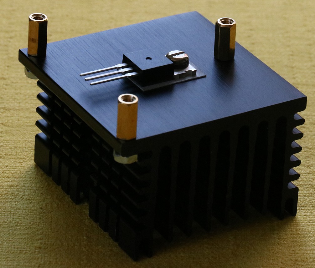 As the most heat will be generated at higher currents and higher voltages – that is what I will focus my testing on. As the MOSFET transistor in use IRL540 will handle >20A current and a power dissipation >150W (
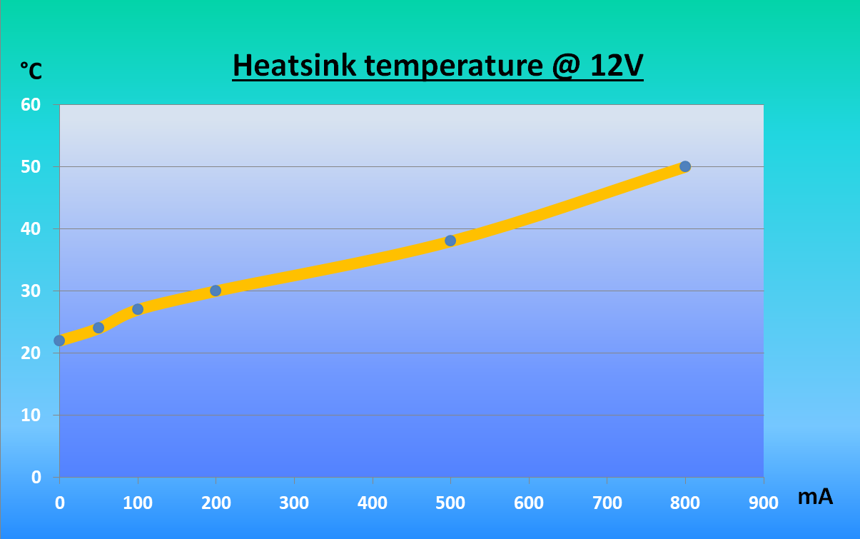


 This is


 Picking the sense resistor is a almost always a compromise. You want the voltage across it to be of a reasonable level for it to not be riddled with electrical noise from the surroundings and at the same time small enough that the heat generated in it will not be too big. If we look at my design as an example: I picked 0.1Ω so 1mA will generate 0.1mV across it. That is very small but is still handled well with the op-amp. 5.7A will generate 0.57V and that turns into 3.2W and that in its turn turns into HEAT! I
  Just a few words about how wonderful op-amps are! 🙂 We want to have a certain amount of
 In case your requirements are totally different to the above it is easy to
  How many Watts the Dummy Load will really be able to handle will depend a great deal on the level of cooling I will be willing to supply – and that I have not decided yet! I do not see that I will ever need a 94W load … but we will see how difficult it is to achieve this! I will probably use a
  That can easily be fixed by using an Arduino for the measuring job and the ESP8266 mainly for presentation and wi-fi. A tempting idea! Another alternative is to add an extra ADC – for example the 4-channel ADS1115. Either solution is roughly the same price ADC or Arduino Pro Mini – just below 2€/$2. An advantage in using an extra separate ADC is that it is higher resolution – 16 bit vs 10 bit! An advantage of using an extra Arduino is it can offload work from the ESP8266. I do not feel I would need the extra resolution in this case!
 To be able to use the dummy load as quickly as possible for the testing of the
 Secondly I automatically measured (at the very same time as above) the output from the DAC with the Arduino 10 bit ADC. That measurement had a slight gain error that I corrected with a standard linear formula. It brought down the deviations to much the same as the multimeter readings – but with generally bigger swings between too high and too low values. Still it is easy to see that both the multimeter and the Arduino ADC have measured the same DAC voltages. So if we squint a little the curves above shows roughly the MCP4725 DAC deviations. Also here I will do something in the software late on.